(Nanowerk Spotlight) Crystalline materials with precisely engineered structures lie at the heart of virtually every advanced technology, from the silicon microchips powering our electronics to the catalysts driving our chemical industries. Crystallization, the phenomenon that transforms disordered atoms or molecules into ordered solid-state structures, is thus a process of immense scientific and practical importance.
However, while researchers have made significant strides in controlling the nucleation of crystals from precursor solutions, directing their subsequent growth to form defect-free single crystals with tailored shapes has proven far more challenging. This limitation has been particularly stubborn for materials like halide perovskites, where controlling the formation of defects results in better photoelectric properties.
Conventional techniques like inverse temperature crystallization or antisolvent vapor-assisted crystallization allow some control over average growth conditions, but their ability to pattern arbitrary single-crystal geometries while suppressing defect formation has remained confined.
Now, a groundbreaking study published in Nature Communications (“Optofluidic crystallithography for directed growth of single-crystalline halide perovskites”) by a team of scientits at at Tsinghua University, may change the paradigm. They have pioneered optofluidic crystallithography (OCL), a radically new approach that leverages a laser as an immensely precise “pen” to simultaneously control the shape and quality of single-crystal halide perovskites as they grow from solution at record speeds.
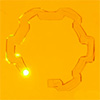
Watch how a laser creates a tiny gear from crystal! This video shows the incredible process of shaping a micro-gear out of halide perovskites using cutting-edge laser technology. (Video: doi:10.1038/s41467-024-48110-w, CC BY)
“The core insight behind OCL is that a tightly focused laser can radically manipulate the local fluid environment around a crystal as it forms,” Xue-Guang Chen, a doctoral student in the Key Laboratory of Advanced Materials (MOE), School of Materials Science and Engineering, Tsinghua University, and first author of the paper, tells Nanowerk. “By tuning laser power and other parameters, we discovered they could generate a spatially confined zone of extreme supersaturation enveloping the crystal, accelerating growth rates to hundreds of microns per second – orders of magnitude faster than even the swiftest bulk methods.”
“Crucially”, he adds, “by dynamically steering the laser beam in two dimensions, this growth can be guided along arbitrary paths, enabling freeform printing of single-crystal structures.”
This level of spatiotemporal control over crystal growth, unprecedented among solution-based techniques, arises from the coordinated action of multiple laser-induced phenomena uncovered through microscopy studies and numerical simulations. Localized laser heating drives both rapid solvent evaporation, intensely concentrating solute, and strong Marangoni convection, directionally replenishing reactants. This synergy creates a self-sustaining, tightly localized supersaturation field that steers crystal growth along the laser’s programmed trajectory with micrometric precision.
The team points out that OCL’s laser-guided growth mechanism opens up a rich parameter space for engineering crystal properties. Varying laser power enabled the team to tune growth kinetics over orders of magnitude, from facet-preserving crystallization driven by gentle supersaturation to rough growth steered by extreme reactant flux.
Judicious selection of surface-binding ligands added a further dimension of control, with optimized concentrations quelling incidental nucleation without inhibiting laser-guided growth. This flexibility to simultaneously modulate growth rate, direction, and morphology distinguishes OCL from traditional methods, which rely on global fluid conditions.
Remarkably, crystals grown by OCL demonstrated exceptional quality, with structural and optoelectronic properties rivaling or surpassing even melt-grown bulk single crystals. Multimodal characterization revealed phase-pure, single-crystalline domains with no detectable grain boundaries, ultra-low defect densities, and intense photoluminescence, attesting to OCL’s ability to print crystals optimized from the atomic scale up. The technique’s versatility was underscored by its compatibility with the major halide perovskite semiconductors, with printed single crystals varying from ultrathin platelets to thick micro-pillars.
Laser-controlled crystallization kinetics. a Schematic showing the spontaneous growth on high-index facets after laser direct printing without surface ligands. b Experimental observation of rapid spontaneous growth on a semicircular pattern created by OCL. c Schematic showing the laser-controlled desorption-adsorption trade-off of surface ligands for precise morphology control. d Optical images showing the printed single-crystal semicircular structure passivated by surface ligands without spontaneous growth. e Schematic showing the laser-induced nucleation at a high concentration of surface ligands and the growth of polycrystalline structure. f Optical images showing the printed polycrystalline semicircular structure without spontaneous growth. Scale bar: 50 µm. g The phase diagram showing the laser-steered crystallization at different optical powers and ligand concentrations (LDPSC: laser direct printing of single crystal; LDPPC laser direct printing of polycrystal). Pth is the optical power threshold of the incident laser, vsp is the spontaneous growth rate, vad and vde represent the ligand adsorption and desorption rate, respectively. h The maximum growth velocity of LDPSC as a function of the surface ligand concentration and the optical power. The shades show the corresponding standard deviation. i The thickness of printed single-crystal halide perovskites using objectives of different NA. The inset panel shows the white light interferometry image of a single crystal printed with an objective of NA = 1.3. Scale bar: 5 µm. The error bars represent the standard deviations. n = 12 independent replicates. (click on image to enlarge)
Looking forward, the researchers anticipate that OCL’s unprecedented control over crystal formation will impact numerous arenas. Its ability to rapidly map composition-structure-property relationships in multidimensional perovskite libraries may transform materials discovery, while the printing of device-integrated single-crystal components could disrupt optoelectronic manufacturing. The prospect of continuous roll-to-roll printing of wafer-scale single-crystal semiconductors further highlights OCL’s disruptive potential.
“Realizing OCL’s full promise will require surmounting remaining hurdles,” Chen cautions. “Our immediate priorities include generalizing the approach to complex oxides, hybrid materials, and other systems where crystal engineering is paramount, as well as addressing scalability bottlenecks through parallelization and automation.”
Nonetheless, by integrating the atomic-scale customizability of liquid-phase synthesis with the equally impressive spatial precision of laser fabrication, OCL offers an enticing paradigm for on-demand single-crystal materials engineered for applications spanning quantum technologies, energy systems, catalysis, and beyond. As researchers build on this powerful demonstration of deterministic crystal growth, a future of bespoke crystalline matter 3D printed from the ground up may be closer than ever.
Get our Nanotechnology Spotlight updates to your inbox!
Thank you!
You have successfully joined our subscriber list.
Become a Spotlight guest author! Join our large and growing group of guest contributors. Have you just published a scientific paper or have other exciting developments to share with the nanotechnology community? Here is how to publish on nanowerk.com.