
Scientists reveal working mechanism of multilayer MoS₂ photodetector with broad spectral range and multiband response

As a typical two-dimensional material, MoS2 exhibits unique optical and electrical properties due to its atomic thickness in the vertical dimension, making it a research hotspot in the field of optoelectronic detection.
The performance of MoS2 devices highly depends on their material characteristics, device structures, and fabrication techniques. Therefore, the photodetection characteristics of MoS2 devices may be determined by various physical effects, which contribute to the development of wideband MoS2-based photodetectors.
A research team from the school of Electronic Science and Engineering of Southeast University has developed wideband MoS2 photodetector, covering a range from 410 to 1550 nm. Through a series of electrical and optoelectronic experiments, the paper reveals the working mechanism of the multiband optical response of the MoS2 device.
The work is published in the journal Advanced Devices & Instrumentation.
In recent years, wideband photodetectors have played an important role in various fields such as optical communication, imaging, transmission, sensing, environmental safety, and monitoring. As a typical two-dimensional material, molybdenum disulfide (MoS2), a transition metal dichalcogenide, has attracted significant attention due to its excellent electrical and optical properties, as well as its ease of processing.
However, the bandgap of MoS2 limits the detection range of its photodetectors. To broaden the response range of MoS2 photodetectors, various chemical treatment methods have been reported. Additionally, integration of MoS2 detectors with photonic nanostructures enables enhanced and broadened light response.
Nevertheless, mechanically exfoliated MoS2 photodetectors prepared without the need for chemical treatment possess irreplaceable advantages. Achieving sub-bandgap photodetection in transition metal dichalcogenides through mechanical exfoliation has become a focus of current research. Furthermore, the performance of two-dimensional material photodetectors is closely related to device structures and fabrication methods.
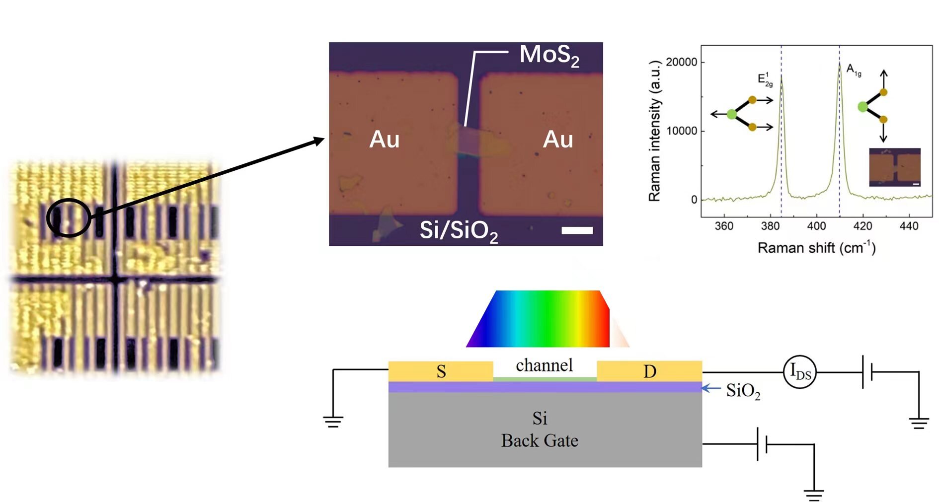
In this study, a multilayer MoS2 field-effect transistor (FET) photodetector was prepared using a mechanical exfoliation method, exhibiting a wide spectral detection range of up to 1550 nm. Experimental results demonstrate that the optimized MoS2 FET exhibits lower resistance and more stable gate control characteristics.
By mechanically exfoliating multilayer MoS2 during the pre-transfer process, high responsivity and specific detectivity were achieved under 480 nm illumination. The device exhibits good output and transmission characteristics under incident light ranging from 410 to 800 nm, and it is photosensitive. The response bandwidth can be extended to 1550 nm, enabling wideband response across multiple spectral regions.
Additionally, the carrier transport characteristics and time-dependent responses of the device at different wavelengths were analyzed. Visible light detection is based on the photoconductive and photogating effects, while infrared light detection beyond the bandgap primarily relies on the photothermal effect.
A research team from Southeast University explained the different electrical characteristics between pretransfer and post-transfer MoS2 devices through the different contact modes between MoS2 and Au. The surface potential difference (SPD) at the MoS2-Au junction of a post-transfer MoS2 device was observed using Kelvin probe force microscopy.
Based on the measurement results of SPD and the difference in work function, it was found that the work function of MoS2 is approximately 0.05 eV smaller than that of Au. The energy band diagram before and after contact revealed the presence of a Schottky barrier at the MoS2-Au interface, which resulted in inferior electrical behavior. In the case of pretransfer devices, the MoS2-Au interface was influenced by Fermi level pinning, leading to a reduction in the work function of Au below that of MoS2. As a result, Ohmic contact was formed at the MoS2-Au interface, reducing the contact resistance and increasing the current.
This study presents an optimized mechanically exfoliated multilayer MoS2 back-gated detector with multi-band photodetection capabilities. Under the optimized pre-transfer fabrication process, the device exhibits improved charge transport performance.
Without the need for chemical treatment, the MoS2 detector achieves a wide spectral photodetection beyond the MoS2 bandgap. The device demonstrates a maximum responsivity of 33.75 A W−1 at visible light (480 nm), with a corresponding specific detectivity of 6.1×1011 cm Hz1/2 W−1. The response mechanism under visible light is attributed to the photogating and photoconductive effects.
Additionally, the device shows a response at 1550 nm infrared light, surpassing the bandgap limitation, which is attributed to the variation in carrier concentration caused by the photothermal effect. The wideband photodetection behavior of the device is attributed to the photoelectric effect in visible light and the photothermal effect in infrared light, providing insights for room-temperature wideband detection and demonstrating significant potential in various fields such as infrared stealth, machine vision, and environmental monitoring.
More information:
Xia-Yao Chen et al, Multilayer MoS 2 Photodetector with Broad Spectral Range and Multiband Response, Advanced Devices & Instrumentation (2024). DOI: 10.34133/adi.0042
Provided by
Advanced Devices & Instrumentation
Citation:
Scientists reveal working mechanism of multilayer MoS₂ photodetector with broad spectral range and multiband response (2024, April 24)
retrieved 24 April 2024
from https://phys.org/news/2024-04-scientists-reveal-mechanism-multilayer-mos.html
This document is subject to copyright. Apart from any fair dealing for the purpose of private study or research, no
part may be reproduced without the written permission. The content is provided for information purposes only.