
Scientists stencil-paint carbon nanotube components for flexible transparent electronics
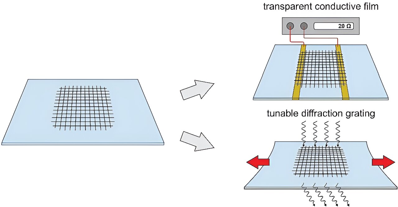
 could serve either as an optical electrode (top right) for flexible transparent electronics or a diffraction grating (bottom right) for 6G communication. Credit: Adapted from Ilya Novikov et al./Chemical Engineering Journal")
Researchers from Skoltech, MIPT, and elsewhere have found a fast and inexpensive way to create geometric patterns in carbon nanotube films. The resulting films turned out to have superior properties for manufacturing components for 6G communication devices and flexible and transparent electronics—such as wearable health trackers. The patterning method is detailed in a paper in the Chemical Engineering Journal.
Like other materials, carbon nanotubes have multiple levels of organization. Down at the atomic level, a single-walled nanotube can be visualized as a 2D sheet of carbon atoms (graphene) rolled into a cylinder. Such cylinders can stick together, forming thicker fibers.
The fibers can interconnect into a vast, porous 3D network, possibly coating some surface as a thin layer—a carbon nanotube film. You can go one step further and modify the film itself, for example by removing some of its material and thus imposing a geometric pattern on it.
“Our team came up with a very efficient way to do this and used it to create a mesh-shaped carbon nanotube film. This used to be achieved by literally burning many holes in a film. The idea is to make the film more transparent at the cost of some electrical conductivity.
“We end up with a transparent conductor that can bend, and that is basically the definition of an optical electrode for flexible transparent electronic devices, such as biosensors that monitor the wearer’s heart rate, breathing, and blood oxygenation,” study co-author Assistant Professor Dmitry Krasnikov of Skoltech Photonics said, adding that the mesh structure can also serve as a diffraction grating—a component potentially useful in 6G signal reception.
As of now, there are two main methods for producing patterned carbon nanotube films. You either make a continuous film and burn holes in it, sacrificing up to 90% of the material, which is clearly not very economical. Or else, really fine lithography has to be used to manufacture the patterned film from scratch.
But that process, too, is fairly expensive and complex, involving multiple steps and the use of liquid solutions, which tend to contaminate the film with impurities and compromise its properties.
“Our approach has a number of advantages,” the study’s principal investigator, Professor Albert Nasibulin of Skoltech Photonics, explained. “It is reproducible, fairly fast and inexpensive, and versatile. No liquid solutions are used, which makes the method cleaner and ensures high quality. In fact, the transparency-conductivity ratio of the mesh—which is its chief figure of merit as far as optical electrodes go—is 12 times better than that of a continuous film.
“On that account, the new technique outperforms fine lithography and is on par with the comparatively wasteful approach where you burn away—and lose!—the extra material. Also, we can create patterns other than meshes, too.”
So how does it work? First the researchers make a copper template of the pattern—in this case a square mesh—by cutting it from copper foil with a laser. They then take a nitrocellulose membrane filter, cover it with the template, and sputter copper particles on it, effectively creating a complementary pattern.
If you then deposit carbon nanotubes on the filter, they will assume the intended mesh pattern, because the sputtered copper repels them. And since the resulting patterned film neither sticks to copper, nor to nitrocellulose, it is easy to transfer to another substrate simply by pressing a piece of rubber, glass, or other material to the filter.
The scientists tested the diffraction properties of the gratings, prepared as 2D meshes on a thin layer of elastic material (elastomer). A terahertz spectrometer clearly registered the diffraction peaks familiar from the optics part of any general physics course, only that those peaks were observed not in visible light but in the THz frequency band, which corresponds to wavelengths of about 1 millimeter and is intermediate between infrared light and microwaves.
The researchers stretched the elastic substrate, thereby varying the grating period, and registered the associated diffraction peak shifts in strict conformity with the known optical laws.
“The ease, simplicity, and relatively low cost of manufacturing structures based on nanotube films, combined with the efficient quasi-optical THz spectroscopy method (using incident THz radiation beam in open space) enable vast opportunities for manufacturing and testing the performance of all sorts of two-dimensional structure based on nanotubes, which could be incorporated in various devices and components using THz radiation,” commented study co-author Boris Gorshunov, who heads the Terahertz Spectroscopy Lab at MIPT.
The team will soon report similar experiments with geometric patterns other than meshes—concentric circles and spirals—for advanced THz imaging. This refers to a safe and noninvasive technology for security screening and medical exams that relies on radiation in the band between microwaves and infrared light.
More information:
Ilya V. Novikov et al, Fast liquid-free patterning of SWCNT films for electronic and optical applications, Chemical Engineering Journal (2024). DOI: 10.1016/j.cej.2024.149733
Provided by
Skolkovo Institute of Science and Technology
Citation:
Scientists stencil-paint carbon nanotube components for flexible transparent electronics (2024, April 23)
retrieved 23 April 2024
from https://phys.org/news/2024-04-scientists-stencil-carbon-nanotube-components.html
This document is subject to copyright. Apart from any fair dealing for the purpose of private study or research, no
part may be reproduced without the written permission. The content is provided for information purposes only.