

TSMC introduces its 1.6nm process with significant performance and efficiency gains
TSMC announced its ground-breaking 1.6nm manufacturing process for chips and it also includes backside power delivery network that improves power efficiency and transistor density even further.

The announced 1.6nm process relies on gate-all-around nanosheet transistors, just like the upcoming N2, N2P and N2X architectures based on the 2nm node. The new process alone allows 10% higher clock speeds at the same voltage and up to 20% lower power drain at the same frequency and complexity. Depending on the chip design, the new 1.6nm process can also fit up to 10% more transistors.
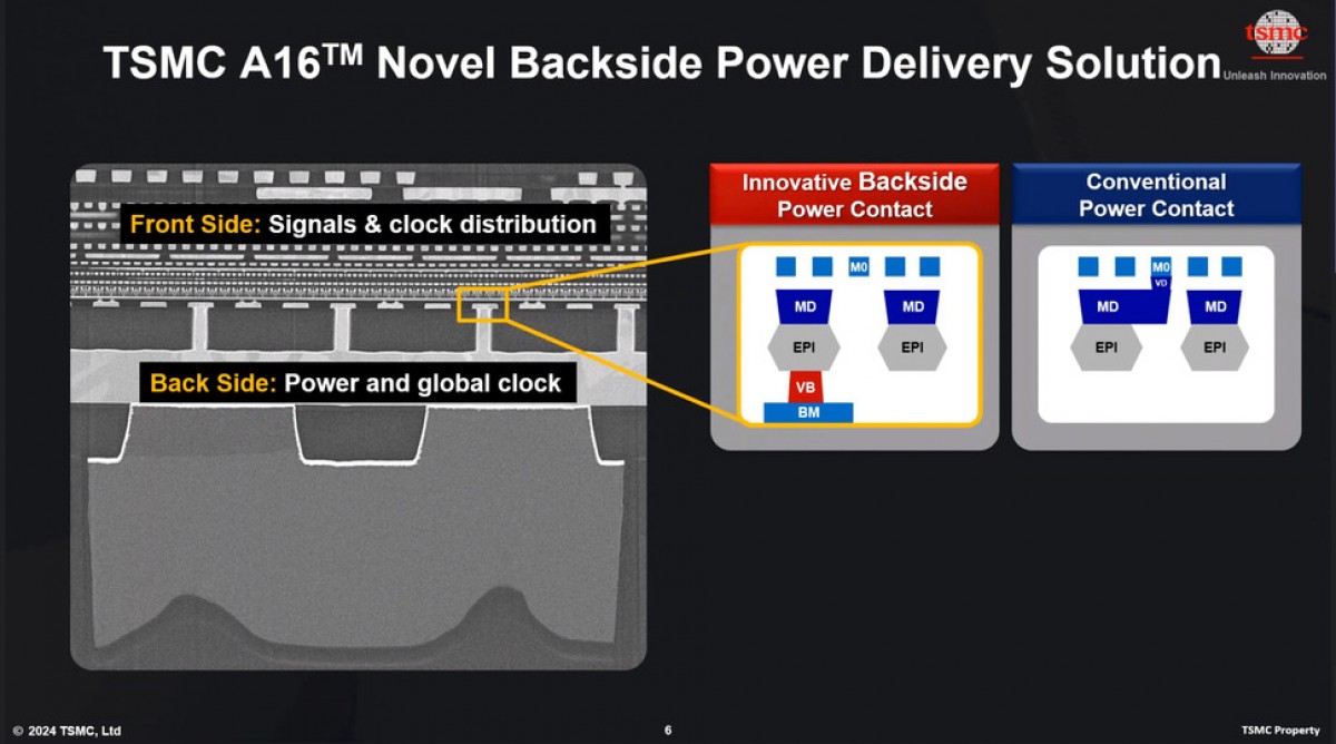
The backside power delivery network is arguably an even more impressive aspect of these future chips as it enables increased transistor density and improved power delivery, which in turn affects performance. TSMC says that along with the Super Power Rail (SPR), which is the type of plug used to conncect the chip to the power source, the backside power delivery network will prove beneficial mostly to AI and HPC processors that require complex signal wiring and dense power networks.
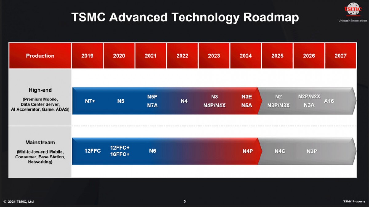
The production timeline is scheduled for the second half of 2026, if all goes to plan, with the first consumer-ready products shipping in 2017.